[ad_1]
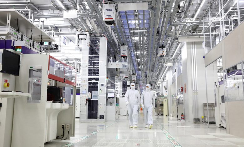
Slicing corners: Samsung’s Texas semiconductor fab was supposed to be a key facility for the mass manufacturing of superior processes beneath 4nm. Nevertheless, a number of setbacks have raised questions on Samsung’s potential to compete within the superior chip manufacturing area. The corporate is quickly shedding floor to TSMC, and until it regains its footing, its decline might considerably influence the semiconductor panorama.
Samsung is dealing with ongoing challenges with 2nm chip yields, prompting the corporate to withdraw personnel from its $17 billion Taylor, Texas plant, which was designed to be a hub for mass manufacturing of superior processes beneath 4nm. This decision, first reported by Enterprise Korea, comes amid repeated delays within the firm’s mass manufacturing timeline, now pushed again from late 2024 to 2026.
Samsung’s foundry yield for processes beneath 3nm at present stands beneath 50 %, with its Gate-All-Round (GAA) expertise yield reportedly as little as 10 to twenty %. In distinction, the superior course of yields at its important competitor, TSMC, stand round 60 to 70 %. In the meantime, Samsung’s chip manufacturing market share is dwindling because the efficiency hole widens, with TSMC holding 62.3 % of the worldwide foundry market, whereas Samsung’s share has dropped to 11.5 %.
High 10 foundries by income (Q2 2024)
| Rating | Firm | Income (2Q24) | Income (1Q24) | QoQ | Market Share (2Q24) | Market Share (1Q24) |
|---|---|---|---|---|---|---|
| 1 | TSMC | 20,819 | 18,847 | 10.5% | 62.3% | 61.7% |
| 2 | Samsung | 3,833 | 3,357 | 14.2% | 11.5% | 11.0% |
| 3 | SMIC | 1,901 | 1,750 | 8.6% | 5.7% | 5.7% |
| 4 | UMC | 1,756 | 1,737 | 1.1% | 5.3% | 5.7% |
| 5 | GlobalFoundries | 1,632 | 1,549 | 5.4% | 4.9% | 5.1% |
| 6 | Huahong Group | 708 | 673 | 5.1% | 2.1% | 2.2% |
| 7 | Tower | 351 | 327 | 7.3% | 1.1% | 1.1% |
| 8 | VIS | 342 | 306 | 11.6% | 1.0% | 1.0% |
| 9 | PSMC | 320 | 316 | 1.2% | 1.0% | 1.0% |
| 10 | Nexchip | 300 | 310 | -3.2% | 0.9% | 1.0% |
| Whole of High 10 | 31,962 | 29,172 | 9.6% | 96.0% | 96.0% | |
To see how far Samsung has fallen behind, one solely has to have a look at TSMC’s Arizona facility, the place recent trial manufacturing has yielded outcomes similar to these of its established crops in Taiwan. The power is on observe to start manufacturing at its first fab within the first half of 2025. The second fab, set to start manufacturing in 2028, will produce chips utilizing 2nm course of expertise with next-generation nanosheet transistors, along with 3nm expertise.
Samsung is now rethinking its technique and has saved solely a skeleton crew on the Taylor plant. The corporate has a preliminary settlement with the U.S. authorities for near $7 billion in subsidies beneath the CHIPS Act, which is now in danger, because the deal requires the plant to be operational.

To be truthful, TSMC’s Arizona facility additionally skilled setbacks in its development and staffing. Nevertheless, Samsung has been unable to resolve its points, regardless of Chairman Lee Jae-yong’s private intervention, together with visits to main gear suppliers like ASML and Zeiss in the hunt for options.
It might be that Samsung’s challenges prolong past technical points. The pervasive paperwork inside Samsung, sluggish decision-making, and low compensation are the primary causes for the decline in foundry competitiveness, a semiconductor professor advised Enterprise Korea. “The delayed funding timing in comparison with 20-30 years in the past additionally signifies that the administration shouldn’t be absolutely conscious of the present actuality, necessitating a elementary overhaul of the administration system,” this individual mentioned.
Samsung’s current struggles are notably placing, given its historical past in semiconductor manufacturing. In 2022, the corporate grew to become the first foundry to realize quantity manufacturing of 3nm chips, outpacing TSMC by practically six months and Intel by a number of years. Samsung had formidable plans to keep up its technological edge by being first to market with 2nm transistors. Nevertheless, it now seems that this purpose could also be out of attain.
[ad_2]
Source