
[ad_1]
In short: Synopsys and TSMC have been working collectively for many years, and a brand new announcement exhibits that they are taking their partnership to the following degree to feed the demand for extra AI computing energy. Synopsys revealed it’s carefully aligning its AI-powered EDA suite and multi-die options with TSMC’s newest course of nodes and 3D packaging tech. The purpose is to pave the way in which for designs packing billions and even trillions of transistors.
For the uninitiated, EDA stands for Digital Design Automation. It is a set of software program instruments for designing digital techniques like built-in circuit chips. On this entrance, Synopsys’ customized design and simulation instruments licensed for TSMC’s N2 node are already paying dividends for MediaTek.
In line with Ching San Wu from MediaTek, the AI-boosted EDA move permits their analog designers to maximise efficiency and effectivity on N2 whereas accelerating the time it takes to ship their SoCs to the market.
Synopsys additionally revealed its bodily verification and implementation options now help bottom routing on TSMC’s A16 course of. A16 is TSMC’s most superior course of node ever, scheduled to be mass-produced within the second half of 2026. Bottom routing is an rising expertise that routes energy provide traces on the bottom of a chip or built-in circuit as a substitute of the standard frontside. This helps optimize energy supply and sign routing for higher efficiency and density.
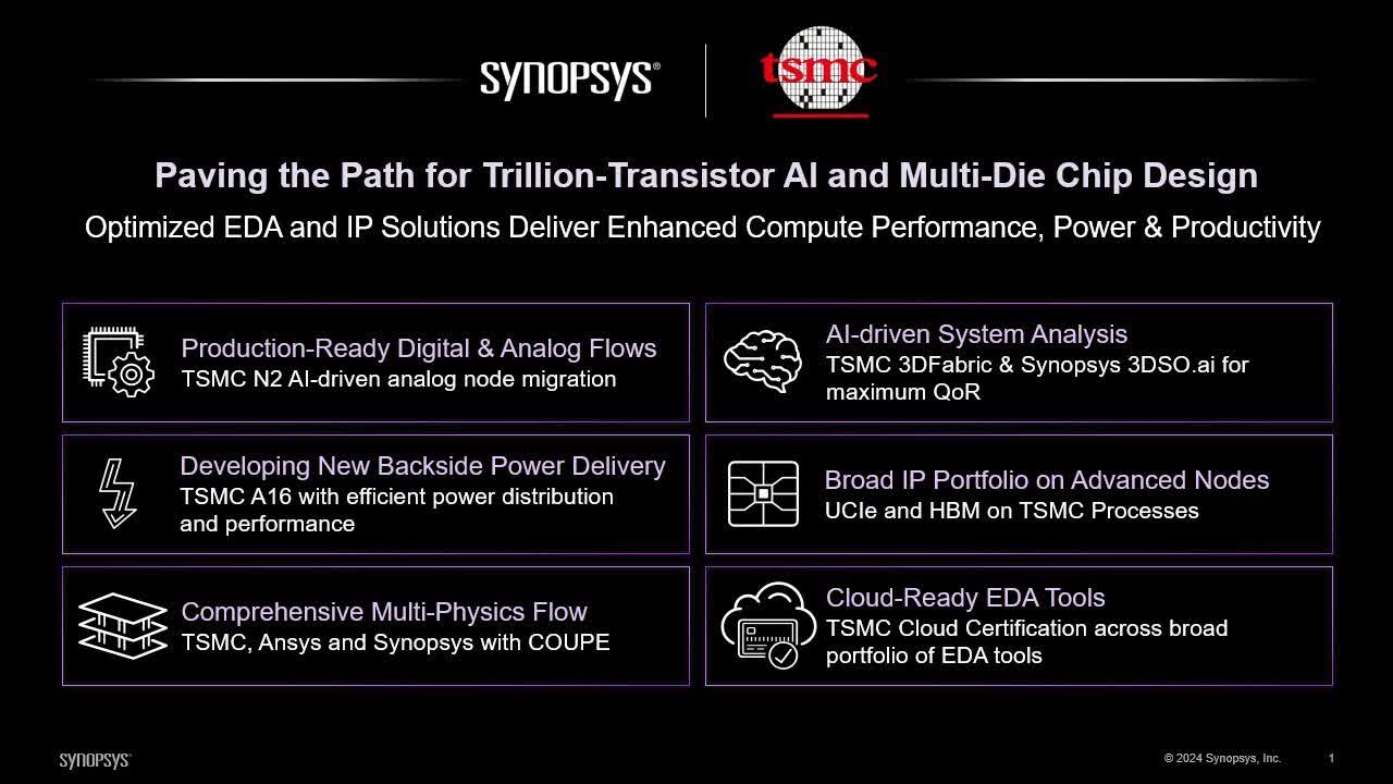
Synopsys provides that its instruments have been cloud-certified by TSMC to additional streamline the design course of. This lets “mutual prospects” faucet into correct cloud EDA assets for duties like synthesis, customized format, simulation, and signoff verification.
On the multi-die entrance, Synopsys’ 3DIC Compiler platform has been enhanced by means of collaboration with Ansys and TSMC. The 3DIC Compiler platform mainly supplies a unified surroundings for designing, implementing, and verifying complicated 2.5D and 3D multi-die packages. With the most recent replace, it performs thermal and IR-aware timing evaluation in tight integration with Ansys’ RedHawk signoff platform.
It is value mentioning that TSMC outlined a roadmap to trillion-transistor chips finally 12 months’s Worldwide Electron Gadgets Assembly (IEDM) convention as properly, adopted by another version in Might. The corporate set 2030 as a goal for 1.4nm A14 and 1nm A10 course of nodes. In parallel, it talked about growing superior packaging applied sciences like CoWoS, InFO, and SoIC. These applied sciences will collectively allow gargantuan multi-chiplet packages exceeding one trillion transistors round 2030. With this new announcement, the chipmaker seems to be shifting nearer to its purpose.
[ad_2]
Source


